Key assessment
Design electrical, thermal and mechanical observability alongside the package, and qualify the complete operating envelope with traceable measurements.
Why packaging has become an architecture question
NIST's 2025 work on advanced semiconductor packaging identifies material needs and measurement challenges as important development areas. The connection is fundamental: a package does more than protect a die. It determines how functions communicate, how power arrives, how heat leaves and what can be measured after assembly.
A working demonstration establishes that an assembly can perform a function under tested conditions. Reliability requires evidence about repeated operation, variation and degradation. When many functions become physically close, a failure can arise from an interaction that was absent during separate component tests. The architecture must therefore reserve ways to observe and distinguish those interactions.
Sources: [1] NIST: material needs and measurement challenges for advanced packaging
Material mismatch creates a coupled problem
Different materials respond differently to temperature and mechanical load. Their interfaces must remain electrically and mechanically useful across the intended environment. The result depends on geometry, fabrication history and constraints, so a single material property is not enough to predict the behaviour of an assembled structure.
Our proposed analysis would track temperature fields, deformation and electrical measurements on compatible timelines. That makes it possible to ask whether a changing resistance precedes a visible defect, follows a thermal transition or varies with a mechanical constraint. Correlation alone is not proof of cause, but time-resolved evidence narrows the experiments needed to distinguish competing explanations.
Measurement changes what can be claimed
A measurement has a detection limit, calibration uncertainty and sampling boundary. If the inspected region is small, the result cannot automatically be extended to every interconnect in a large package. If the test observes only external pins, internal faults may produce similar symptoms and remain difficult to localise.
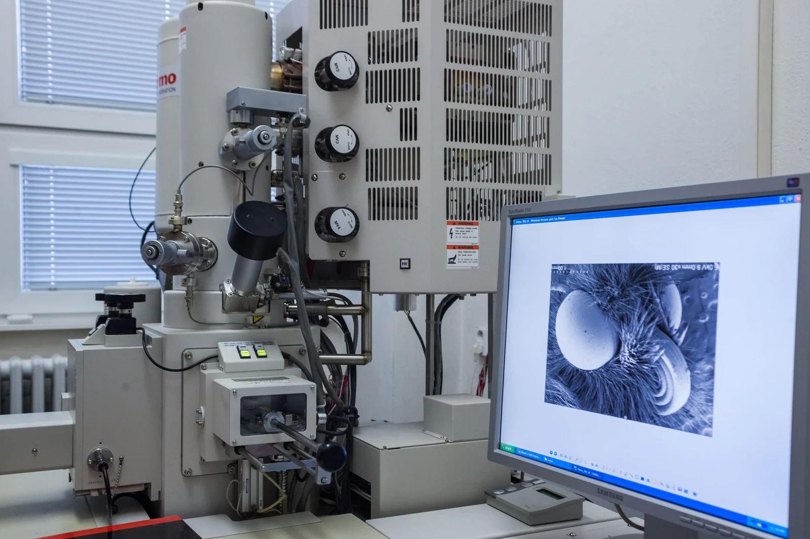
We would define the claim before selecting the instrument: minimum detectable change, spatial coverage, relevant time scale and acceptable uncertainty. The instrument should then be matched to that claim. An attractive microscope image may help explain a structure, but it is not a substitute for a documented method that can quantify the failure mode across a representative population.
Qualification needs a stress map, not one extreme
A useful stress programme connects expected operating conditions to credible degradation mechanisms. Temperature, activity, current and mechanical loading may interact; testing each at an unrelated extreme can either miss the relevant coupling or create a failure that is not representative. The relationship between accelerated tests and intended operation should be stated rather than assumed.
Acceptance should distinguish initial performance, drift within specification and functional failure. That requires defined thresholds and a plan for censored observations, where a sample has not failed by the end of a test. A claim about lifetime needs more than the survival of one sample: population size, exposure history and uncertainty determine how strong the inference can be.
Traceability makes failures reusable
A package investigation becomes far more useful when each measurement is linked to material batches, process versions, assembly sequence, calibration and software configuration. Without those records, a later failure may look new even when it repeats a known condition. Traceability turns a component incident into evidence for the next design and qualification cycle.
The public NIST packaging programme provides a framework for the importance of these capabilities. Our engineering interpretation is that test access and provenance should be budgeted early, alongside bandwidth and power. Treating measurement as an optional final-stage expense can leave a high-performance system that is difficult to debug, qualify or improve.
Sources: [3] NIST: advanced packaging manufacturing programme
COTT assessment
Advanced packaging succeeds when integration remains observable and controllable. The most persuasive evidence connects a physical structure to electrical function, thermal behaviour and repeatable manufacturing outcomes. Those links enable a team to explain a failure instead of merely replacing a component until the symptom disappears.
For our technology perspective, the priority is a complete validation boundary: what was measured, under which conditions, with which uncertainty and across which population. That is a practical bridge between microelectronics and system engineering. This article is a sourced technical review, not an assertion that COTT operates the depicted laboratory or has completed a proprietary packaging qualification.
Primary sources & method
[1] NIST: material needs and measurement challenges for advanced packaging[2] NIST: semiconductor metrology programme[3] NIST: advanced packaging manufacturing programmeSources checked 2026-10-11. COTT Electronics editorial analysis of published evidence. Reported experimental results are attributed to their original teams; illustrative calculations and our assessments are identified in the text.
This is a technical editorial review, not an externally peer-reviewed paper or a report of original COTT laboratory results.